In essence a relay is an electric switch. It uses power and an electromagnet to close a switch.
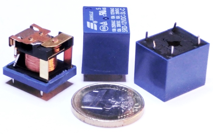
This relay has five connections as shown in the picture below.
This can be simplified by letting out the ground pin, so a simple four pin scheme is obtained. There are four basic switching possibilities for a relay, depending which contacts are powered. Green is power that switches the relay, red is power that is switched and black is no power. This relay is a Single Pole Double Throw relay, as shown in the figure below right.
 |
Source: Wikipedia |
Since computers use binary data, signals are very simple: 0 (no voltage) or 1 (voltage). In MERCIA’s case 12V relays are used because this voltage is not too low to have large amperage's and not too high to have problems with dissipating the power for the used LED’s.
A combination of several relays can realize almost every function that can be found in a relay computer. However, in a number of cases it is more efficient to use one or more diodes. Since (flyback) diodes are also necessary to protect the LED’s that connected parallel to the relay and diodes play an important role in the memory implementation, I choose to incorporate diodes into the designs.
There are a number of functions that are used on one or more places in a relay computer. I’ve called these functions ‘elements’. In the following paragraphs I’ll describe these elements.
Relay logic
The relay logic of a bare relay is given in the truth table below.
|
In |
Out |
In |
Out |
|||||
|
Coil |
CO |
NC |
NO |
Coil |
NC |
NO |
CO |
|
|
0 |
0 |
0 |
0 |
0 |
0 |
x |
0 |
|
|
0 |
1 |
1 |
0 |
0 |
1 |
x |
1 |
|
|
1 |
0 |
0 |
0 |
1 |
x |
0 |
0 |
|
|
1 |
1 |
0 |
1 |
1 |
x |
1 |
1 |
|
The relay can be used in two way’s, depending if the CO or NC/NO are used as input (figure left).

For the connections between the relay pins an uniform color code will be used (above figure right) in all my relay circuit diagrams. This makes it possible to determine the function of a line by its color.
Basic binary logic
Three basic logical functions are known: AND, OR and XOR. If there is a N in the function name, the output will be inverted (NOT). That means 1 becomes 0 and 0 becomes 1. This is shown in the table below.
|
In |
Out |
|||||||
|
a |
b |
AND |
NAND |
OR |
NOR |
XOR |
XNOR |
|
|
0 |
0 |
|
0 |
1 |
0 |
1 |
0 |
1 |
|
0 |
1 |
|
0 |
1 |
1 |
0 |
1 |
0 |
|
1 |
0 |
|
0 |
1 |
1 |
0 |
1 |
0 |
|
1 |
1 |
|
1 |
0 |
1 |
0 |
0 |
1 |
AND and NAND gates
The output of an AND gate will only give 1 when both inputs are 1. For a two input port, only one relay is needed. For every extra input one extra relay is needed. Another relay is used to invert the signal.
OR and NOR gates
Just connecting the lines together, can create an OR gate. However, if an input becomes 1, all the other inputs – even if they are 0 - will also become 1. This can create unwanted feedback to relay’s earlier in the switching chain. This problem is eliminated by adding diodes, as shown with the red lines in the picture below. Then the signal cannot be fed back to the other inputs. For a NOR port, an inverting relay is added.
For the purists among us, the OR and NOR gates can also be realized with the use of relays only as shown in the following circuit diagram.
XOR and XNOR gates
The most elegant way to create a two input XOR gate, is the use of two relays with crossed connections as shown below. Only when one of the inputs is 1, the output will be 1. An inverter will make the XOR a XNOR gate.
A XNOR can also be created using only two relays, as shown in the circuit diagram below.
An entirely different approach is needed for a XOR gate with more than two inputs, as shown in the next circuit diagram.
The first two relays to the left form a triple AND-gate. The diodes will feed one or more 1-es to the output. The third relay forces the output to 0 when the AND-gate is true. The last relay (to the right) is used to invert the signal.
Another solution for the XNOR gate uses two more diodes but only three relays.
One bit only
In some cases it is required to have only one of four signals different. This is given in the truth table below. Besides the already presented AND/NAND and OR/NOR there are two specials: Special 1 and Special 2.
|
|
|
|
Only one 1 |
|
Only one 0 |
||||
|
In 1 |
In 2 |
|
NOR |
Sp1 |
AND |
|
OR |
Sp2 |
NAND |
|
0 |
0 |
|
1 |
0 |
0 |
|
0 |
1 |
1 |
|
1 |
0 |
|
0 |
1 |
0 |
|
1 |
0 |
1 |
|
0 |
1 |
|
0 |
0 |
0 |
|
1 |
1 |
1 |
|
1 |
1 |
|
0 |
0 |
1 |
|
1 |
1 |
0 |
These functions can all be implemented with the use of only one relay, except the OR (no relays) and the NAND (two relays). The circuit diagrams for the first 5 functions are given below.

Universal Logic Unit
An universal logic table can be implemented using three relays as shown in the following (left) relay circuit diagram.

The required function is coded with the lines L1 to L3. For instance when an AND is needed L3 must be set to 1 and when a XNOR is needed L1 and L3 must be set to 1. The right diagram shows how this principle can be used to make a universal logic port. The lines top left are used to select the required function.
An implementation of a Universal Logic Unit is shown below. Here switches are used to select the required port. An extra option is added with the fourth switch, that enables a set-reset flip-flop


Value trigger
The purpose of a value trigger is to switch a relay when a number of lines has a predefined value. In the circuit diagtram below, three XNOR gates connected by an OR-gate are shown. When the switches are set as shown in the schematic, the output relay will only switch off, when all the three input lines are 1. This resembles a NAND-gate. When the NC of the output relay instead of the NO contact is used, the value trigger behaves as an AND-gate. If the three switches are all toggled, then the output relay will switch on when one of the input relays contains a 1. This resembles an OR-gate. If for instance only S2 is toggled, only the input 101 will result in the output 0.
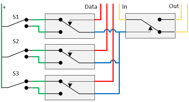
If required, the switches can also be replaced with relays or signals, and than the value trigger can be configured by signals.
Switch
The purpose of a switch is to connect or disconnect lines. The truth table is very simple and resembles that of an AND-gate. The switch works both ways, so the output can also be the input.
|
Enable |
In |
Out |
|
0 |
0 |
0 |
|
0 |
1 |
0 |
|
1 |
0 |
0 |
|
1 |
1 |
1 |
Amplifier
Relays are often put behind each other. This can be called a relay switching chain. It is important to know the switching chain. Below a switching chain, with a switching depth of two and a switching width of three.
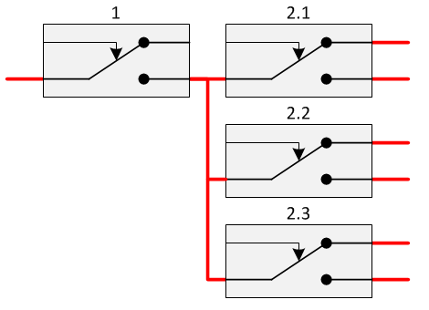
The switching depth is defined as the number of relays that are placed behind each other. This is an important factor to determine the clock-speed of the relay computer. The larger the switching depth, the lower the allowed clock speed. The switching width is defined as the number of relays that are switched by a certain relay. The switching width of relay 1 is three. This is important for the maximum allowed currant that may be switched by a relay. It is essential that the switching width stays well below the allowed switching amperage. This will significantly increase the lifetime of the relays. In the circuit diagram below left, an amplifier is drawn. Note that the amplifier will only work in one direction.
An amplifier can be used to reset the switching width to 0, however it will increase the switching depth with one.
The schematic on the right shows an amplifier that will not increase the switching depth. It can be used to bring up the voltage to 12V again.
Switch and amplifier combined
In a number of occasions, it can be very useful to combine the on-off switch and the amplifier. This can easily be done by adding just one relay, as shown below.
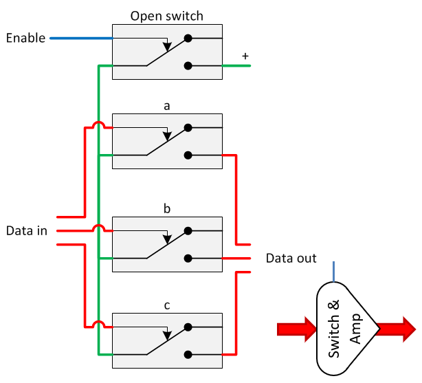
Also this circuit will only work in one direction.
Decoder
The purpose of this decoder is to convert a binary word of n bits to the 2n separate signal lines. Herefore 2n – 1 relays are needed. The decoder will only have output, when the enable signal is set to 1. This is drawn in the next circuit diagram.
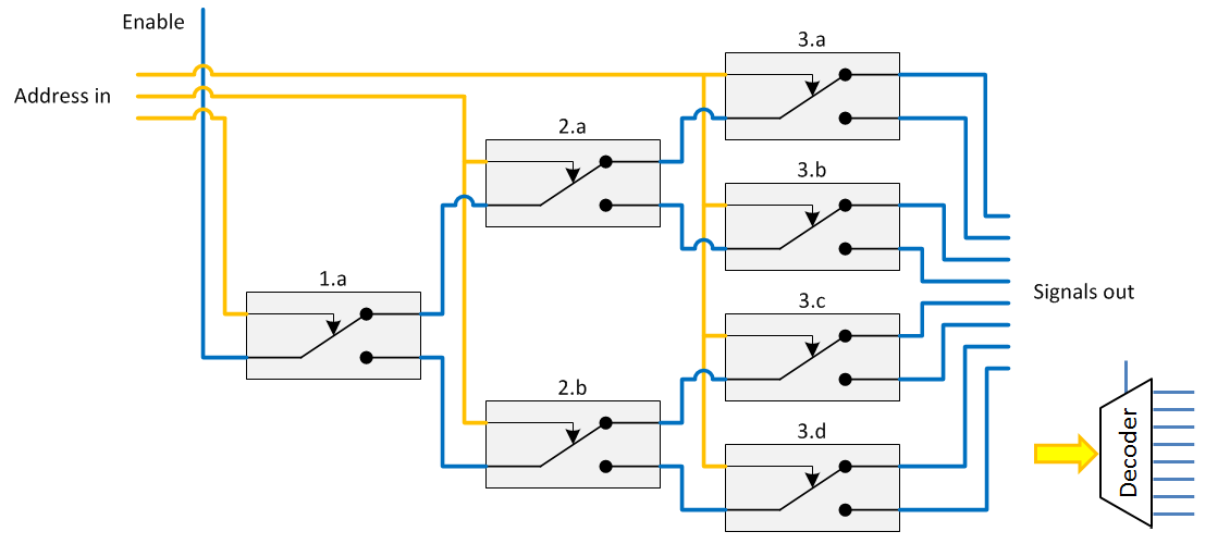
A decoder is an important part of memory addressing.
Encoder
The encoder does the opposite of the decoder. It converts a number of disjunct lines (XOR function, only one of the lines contains a 1) to a binary word. A special form of the encoder is the universal encoder. In that case the coding is done with the use of DIP-switches. A universal encoder can also be used as ROM (Read Only Memory).
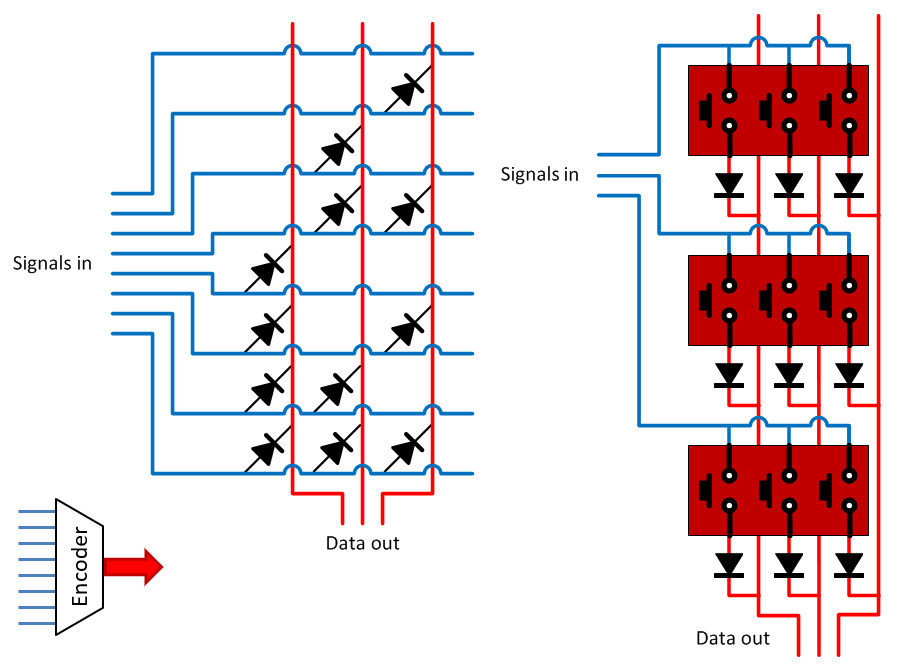
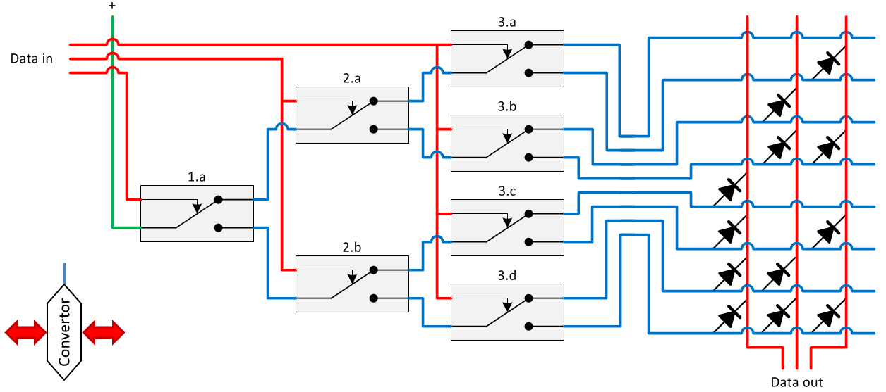
Convertor: encoder and decoder combined
A combination of a decoder followed by an encoder can be used to do bit transformations from input to output. This is for example used to convert a 4-bit integer (4 bit in) to a 7-segment display code (7 lines out). The principle is shown below, with a (useless) example where the output is identical to the input.
Sending disjunct signals
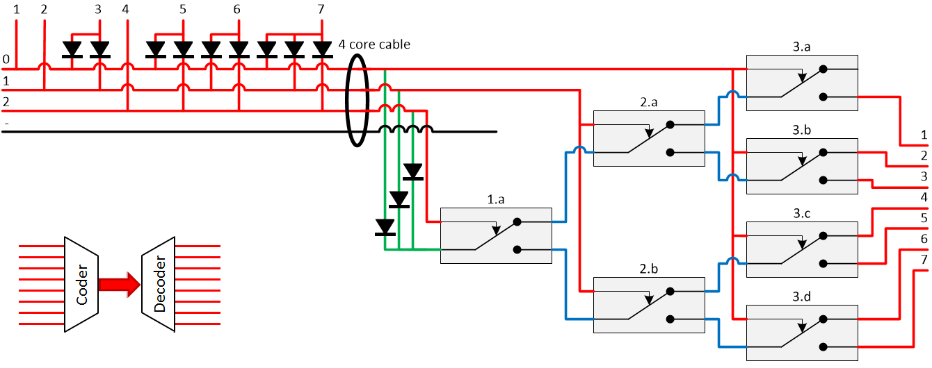
The following circuit can be used to steer two disjunct (only one signal at the time is active) signals over a two-core cable. The used trick is to switch polarity of the two lines and use diodes to detect polarity. The first signal switches polarity and uses a delay relay to send the signal after the polarity has been changed. The second signal leaves the polarity intact and only sends the signal.

For three or more signals, a convertor or the combination of an encoder followed by a decoder is used. For 3 signals a 3-core cable is needed. A 4-core cable can transport 7 disjunct signals. This is shown in the schematic below.
Multiplexer
The purpose of a multiplexer is to select one out of a number of inputs. A multiplexer is in principle a combination of a decoder and a switch. There are two implementations possible: one that uses a decoder for every input and one that uses a decoder and a switch for every input. Both circuit diagrams are given. The given situation: number of inputs and number of bits determine which of both possibilities consumes the least number of relays. When the first input (Data 1) is not connected and both decode bits are set to 0, there will be no connection between in- and output. In the following circuit diagram, ‘Data in 1’ is (default) connected to the output when both decode bits are set to 0.
Latch
A latch is a circuit that will hold (remember) the logical 1’s of the input until it is cleared. The circuit diagram for a 3-bit latch is shown below.
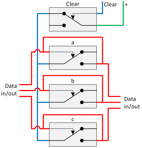
The truth table of a latch is given in the next table.
|
Register |
Input |
Register |
|
|
before |
Clear |
In |
after |
|
0 |
0 |
0 |
0 |
|
0 |
0 |
1 |
1 |
|
0 |
1 |
0 |
0 |
|
0 |
1 |
1 |
0 |
|
1 |
0 |
0 |
1 |
|
1 |
0 |
1 |
1 |
|
1 |
1 |
0 |
0 |
|
1 |
1 |
1 |
0 |
Register
When a latch and switches are combined, a register emerges. Registers do play an important role in computers. They store bytes in a more accessible way than memory does. In the 3-bit circuit diagram below, the latch is combined with two switches. This is often done to be able to connect the register to a data- as well address-bus.
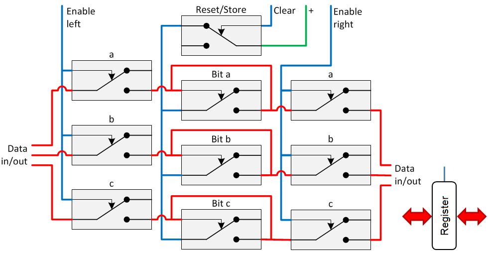
In a number of occasions, for copying values, in a relay computer two registers are connected together. It is important to understand that registers cannot be copied, in that sense that there is a source and a destination, and the destination register will get the source values regardless of what the current values are. Both registers will connect and take each other’s values through an OR-function.
This is given in the following truth table. Left of ‘Enable’, the values of a bit in the registers before connecting them, right the values after connecting them.
|
Reg 1 |
Reg 2 |
Enable |
Reg 1' |
Reg 2' |
|
0 |
0 |
Ò |
0 |
0 |
|
0 |
1 |
Ò |
1 |
1 |
|
1 |
0 |
Ò |
1 |
1 |
|
1 |
1 |
Ò |
1 |
1 |
R/W Register
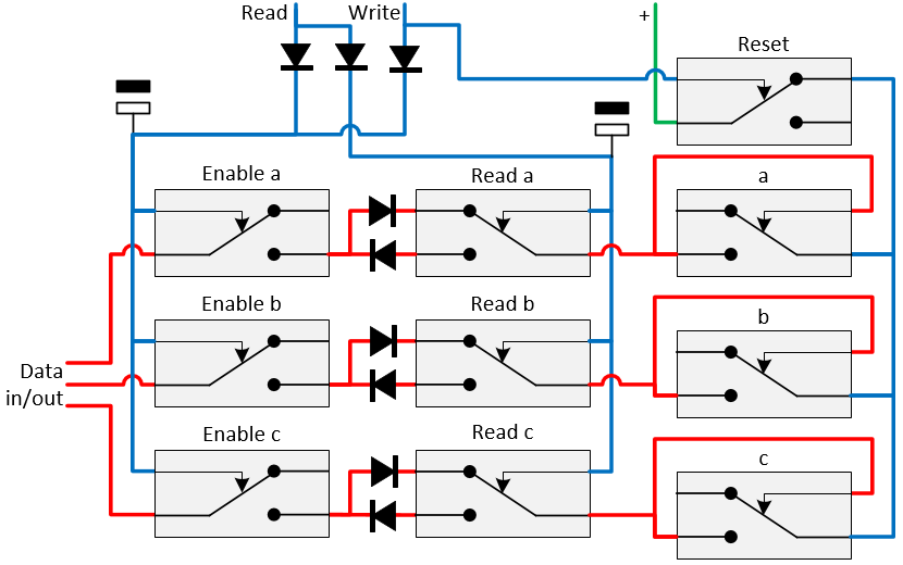
The OR-problem with registers can also be solved by the construction of a Read/Write register. Diodes enforce that the bits are read or written. During the read the enable and read relays are set to 1. During the write, the enable and reset relays are set to 1. In order to prevent that bits got lost when the read signal drops from 1 to 0, capacitors are used which will hold the enable and read relays a bit longer than the reset relay.
Radio button
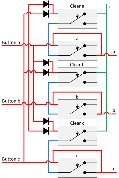
A so-called radio button is a set of buttons, only one of which can be selected at any time. This can be implemented using n*2 relays and n*(n-1) diodes. Beneath an example for three radio buttons is given. In essence it uses a latch with corresponding clear relay for every button. When a button is pressed, a signal is given to the corresponding latch to activate and to all other clear relays to clear the other latches.
Pulse generators
A relay in combination with a capacitor can also be used to generate pulses. The circuit diagram to the left shows a single pulse generator. A trigger signal causes a pulse to be given, the duration depends on the capacity of the capacitor. F=A*V/s or the required capacity in Farad is determined by the relay its current in Amperes multiplied by the Voltage of the relay divided by the required pulse length in seconds.
The circuit diagram to the right shows the generation of a (asymmetric) pulse train. Here the frequency is determined by capacitor capacity. Bear in mind that the capacitor must activate both relays, so the current is twice the current of a single relay. When a symmetric pulse train is needed, a T flip-flop must be connected to pulse output.

Delay line
Delayed switching is very useful when registers are used. A register is often put at the end of a relay switching chain. Unless the last relay switched, the value of the chain is undefined. This is shown in the next two examples. The top circuit will put a 1 in the register, while the bottom circuit will not.
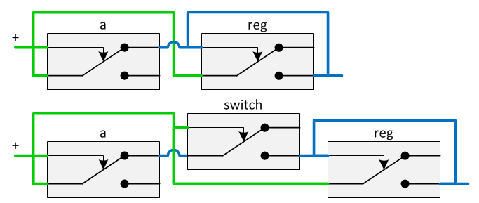
In order to avoid these kinds of problems, the register must only be enabled when all the switching has been done. For a switching chain with length n and a relay switching time of t, this is after a delay of n*t. Therefore, a delay-line with a delay-time of n*t.
This can be solved by n relays put in a switching chain (top circuit diagram). A more elegant solution can be found in the circuit diagram at the bottom. There a capacitor is used to realize the required delay. As usual, the mass connection of the capacitor is not drawn (but is needed). The capacity of this capacitor must be chosen precisely, so that the required delay is achieved.

It is important to realize that after each usage of this delay-line, the capacitor must be given some time to recharge. An delayed off can be realized with the following circuit.
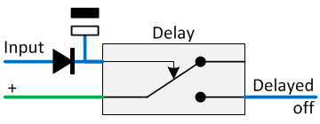
Both circuits, delayed on and delayed off, can also be combined by placing the delayed off circuit behind the delayed on circuit.
SR flip-flop
The Set/Reset flip-flop or SR flip-flop is the base for a register. It can be constructed using four relays. ‘Clock’ will enable both the set and reset lines. ‘Set’ will set the flip-flop to 1, ‘Reset’ to 0. The two relays to the left are used to enable the lines. The Bit store relay below right, is the relay that stores the bit by the use of a feedback line from ‘Q’ to the coil. The Inverter relay provides the power to the Bit store relay. When activated, it cuts the power.
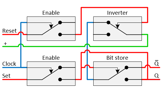
D flip-flop
The Data flip-flop or D flip-flop is an extension of the SR flip-flop. When the ‘Clock’ signal is given, the value of the ‘Data’ line is stored. ‘Set’ will set the flip-flop to 1, ‘Reset’ to 0. ‘Clock’ will give the flip-flop the value the ‘Data’ has. The function of the two relays on the right is the same as the SR flip-flop. The Enable relay enables ‘Data’. The Delay relay is important when the ‘Clock’ goes to 0. First, power is provided to the bit store relay, then ‘Data’ line is cut off from the bit store relay. This sequence is enabled by the delay relay.
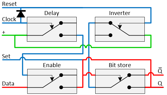
T flip-flop
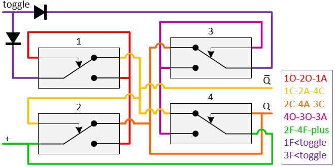
The Toggle flip-flop or T flip-flop will divide an input pulse train by two. E.g. every even pulse will bring the output to 1, every odd pulse will return the output to 0. The relay circuit diagram for this flip-flop is given below. The wire coding is given in the table to the right. An explanation of the wire coding conventions can be found in the last paragraph. To make the construction more visible, several colors for the connection wires where used.
The ‘inverse Q’ is not clean, during the switching there is a short moment that both the ‘Q’ and the ‘inverse Q’ will be 1.
The way this circuit diagram works is quite complicated. In order to clarify the working, the switching sequence is shown below.
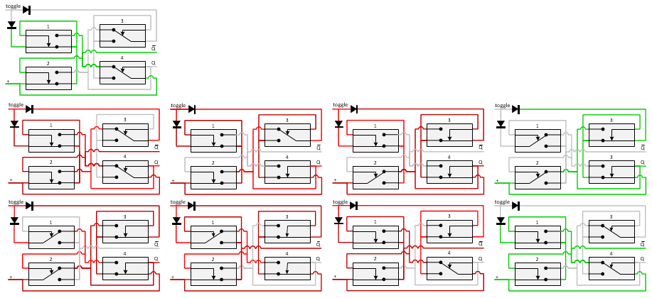
Adder
An adder ads two binary numbers. The addition of two binary values is defined by the following truth table. The output of an adder, called the result, can be obtained by the logical function a XOR b.
|
Half adder (incrementer) |
|||
|
In |
Out |
||
|
a |
b |
result |
carry |
|
0 |
0 |
0 |
0 |
|
0 |
1 |
1 |
0 |
|
1 |
0 |
1 |
0 |
|
1 |
1 |
0 |
1 |
The carry is the value that has to be taken to the next bit to the left, which is the more significant bit. So every bit has an incoming carry from the right (less significant bit) and an outgoing carry to the left (more significant bit). The carry can be obtained by the logical function a AND b. An adder that is calculating the sum from only two inputs, is called a half adder. Half adders are also known as incrementers, since they can add 1 to a binary number. The circuit diagram is given below left.

It is possible to combine the first XOR port and the AND port in one relay, saving a relay. This circuit diagram is shown above right.
When the carry bit of the less significant bit is taken into account, there are three inputs: a, b and the carry. An adder that can handle these three inputs is called a full adder. The following truth table is applicable to a full adder.
|
Full adder |
||||
|
In |
Out |
|||
|
Carry |
a |
b |
c |
Carry |
|
0 |
0 |
0 |
0 |
0 |
|
0 |
0 |
1 |
1 |
0 |
|
0 |
1 |
0 |
1 |
0 |
|
0 |
1 |
1 |
0 |
1 |
|
1 |
0 |
0 |
1 |
0 |
|
1 |
0 |
1 |
0 |
1 |
|
1 |
1 |
0 |
0 |
1 |
|
1 |
1 |
1 |
1 |
1 |
A full adder can be realized by the combination of two half adders. One that adds a and b and one that adds this result with the carry. The circuit diagram - a full adder with only four SPDT relays - is given below.

The term ripple carry is used when the value of the carry out is calculated by use of a relay that is switched on by the carry in. In that case the carry ripples through the entire word and causes a significant delay. With Mercia’s ten-bit word, this means that in a worst case 10 relays must be consecutive switched on, before the carry of the most significant bit (MSB or bit 9) is calculated correctly.
It is evident that a ripple free adder is needed in order to eliminate the carry delay. Therefore an ALU is used instead of an adder. This ALU is described here: Relay ALU. When the shift right relay is left out, this ALU can also be used as a six relay ripple free adder.
BCD adder
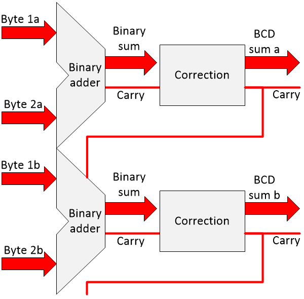
A relay-based BCD adder is an adder who ads two binary coded decimal (BCD) numbers. The principle is given in the schematic below. It is a regular adder followed by the logic to correct the binary sum as well as the carry. A 4-bit binary number counts up to 15, a 4-bit BCD number to 9. The correction logic generates a carry and corrects the value down to a value below 10. The binary adder has been described in the previous paragraph.
The maximum number that must be corrected is 9 + 9 + 1 (carry) is 19. The way the value and carry should be corrected is given in the table below.
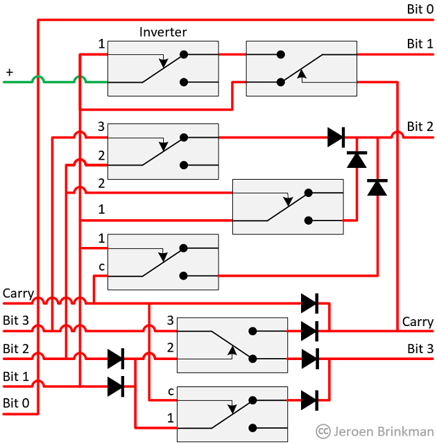
This can be archived by the following logic:
Cout := (bit3 AND NOT(bit2 OR bit1)) OR Cin
bit3 := (bit3 AND (bit2 OR bit1)) OR (Cin AND bit1)
bit2 := (bit 1 AND bit 2) OR (bit 2 AND NOT bit3) OR (Cin AND NOT bit1)
bit1 := (bit 1 AND NOT Cout) OR (Cout AND NOT bit1)
bit0 := bit0
This logic is implemented in the following circuit diagram.
For every BCD byte one adder and one logic block is needed. The total number of relays counts up to (4 * 6) + 7 = 31 or almost 8 relays per bit.
Comparator
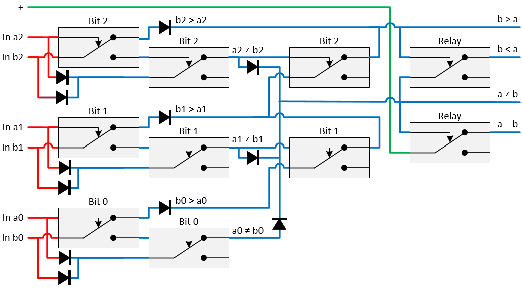
The comparator will take two binary values and compare them to decide if they are equal, greater, less or unequal. The leftmost relais detects if the b-bit is high and the a-bit low (also see one bit only). The relays in the second column create a XOR function. When Ax does not equal Bx, then it is clear if Ax is greater than Bx or vice versa. When they are equal, then the decision must be made based on Ax-1 and Bx-1 level bits. This is done by the relays in the third column. Since there are diodes in the circuit, the results of the bitwise comperation can be OR-red by connecting the lines together. The rightmost relays invert the results.
Relay wire coding
In order to convert the circuit diagrams to working PCB's, relay wire coding can be very helpful. It is used to implement relay circuit diagrams and check the implemented wiring.
The pins of a relay can be coded as follows:
A – Activate relay
F – Feed
C – commonly Closed
O – commonly Open
G – Ground
Consider the following circuit diagram that is called ‘fake function’

The connections can be coded in the following two ways:
Fake circuit:
1A – 1C
1O – 2C – 2A or 1O – 2C, 2C – 2A or 1O – 2A, 2A – 2C
1F – plus
2O > out
or
Fake circuit:
Red: 1A – 1C
Yellow: 1O – 2C – 2A or 1O – 2C, 2C – 2A or 1O – 2A, 2A – 2C
Green: 1F – plus
Blue: 2O > out
Use the following conventions:
- The coding starts with the function name of the circuit diagram.
- Every relay has a number.
- Every line starts with the color name or the line is printed in the applicable color.
- Every line is a continuous connection, e.g. all the pins mentioned on the line are connected to each other.
- A connection is indicated by “-“
- A diode is indicated by “>”, marking the direction the diode is conducting.
- Relay pins in upper case and other signals in lower case.
- Black: G1 – G2 – minus, is considered trivial and therefore left out.
December 2020, Jeroen Brinkman


