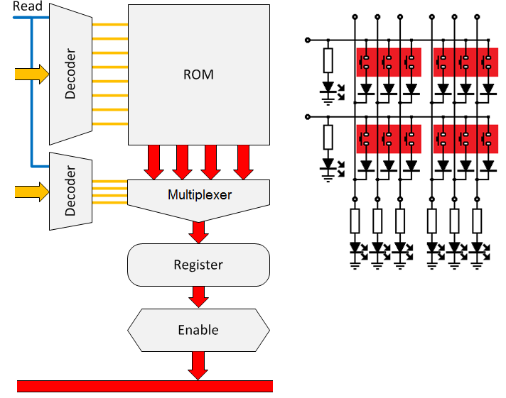
The Mercia memory consists out of three types of memory:
- ROM: first there is the Read Only Memory or ROM, implemented with DIP-switches;
- RAM: secondly there is Random Access Memory or RAM, implemented with capacitors and
- ReM: third there is zero page Input/output or I/O RAM, implemented with relays.
The MERCIA relay computer is a 10 bit computer. This makes possible to address 1K or 1024 bytes of memory with a single word. For the purposes Mercia is will be used, 1K of memory seems to be sufficient. As a result of that no two word memory addressing is needed, but a single word memory addressing suffice.

Memory mapping
The format of a memory address is: t ccc pp bbbb
|
t |
is the type of memory, 0 is ROM and 1 is RAM |
|
ccc |
is the bank or column number for one of the eight columns: 000 to the left and 111 to the right |
|
pp |
Is the PCB number for one of four PCB’s: 01 at the top and 11 at the bottom |
|
bbbb |
is the address of the byte on the PCB: 0000 at the top and 1111 at the bottom. |
The memory uses addresses (rows) and banks (columns). The memory banks are implemented vertical, the memory addresses horizontal. As can be seen in the table below, for 512 bytes the optimum is to use 64 addresses (rows) and 8 banks (columns).
|
Rows*Culums |
Relays |
||||
|
512 |
Addresses |
Banks |
Addresses |
Banks |
Total |
|
1 |
2 |
256 |
1 |
2550 |
2551 |
|
2 |
4 |
128 |
3 |
1270 |
1273 |
|
3 |
8 |
64 |
7 |
630 |
637 |
|
4 |
16 |
32 |
15 |
310 |
325 |
|
5 |
32 |
16 |
31 |
150 |
181 |
|
6 |
64 |
8 |
63 |
70 |
133 |
|
7 |
128 |
4 |
127 |
30 |
157 |
|
8 |
256 |
2 |
255 |
10 |
265 |
|
9 |
512 |
1 |
511 |
0 |
511 |
|
10 |
1024 |
0,5 |
1023 |
-5 |
1018 |
The above combination of addresses and banks leads to the following memory mapping.
|
0 |
000 |
001 |
010 |
011 |
100 |
101 |
110 |
111 |
|
00 |
1/O |
ROM 1 |
|
ROM 5 |
||||
|
01 |
ROM 2 |
ROM 6 |
||||||
|
10 |
ROM 3 |
ROM 7 |
||||||
|
11 |
ROM 4 |
ROM 8 |
||||||
|
1 |
000 |
001 |
010 |
011 |
100 |
101 |
110 |
111 |
|
00 |
RAM 1 |
RAM 5 |
RAM 9 |
RAM 13 |
||||
|
01 |
RAM 2 |
RAM 6 |
RAM 10 |
RAM 14 |
||||
|
10 |
RAM 3 |
RAM 7 |
RAM 11 |
RAM 15 |
||||
|
11 |
RAM 4 |
RAM 8 |
RAM 12 |
RAM 16 |
||||
Making the memory work
There are three commands for the memory:
1. clear the memory (not applicable for ROM);
2. write the memory (not applicable for ROM);
3. read the memory.
The computer does not know what memory it is using, so the memory control is exactly the same for the three types of memory. The control timing is given in the next figure: horizontal the signal lines, vertical the actions.
|
|
|
clear |
|
|
|
|
write |
|
|
|
read |
|
|||
|
Clear |
|
|
|
|
|
|
|
|
|
|
|
|
|
|
|
|
|
|
|
|
|
|
|
|
|
|
|
|
|
|
|
|
|
Write select |
|
|
|
|
|
|
|
|
|
|
|
|
|
|
|
|
|
|
|
|
|
|
|
|
|
|
|
|
|
|
|
|
|
Address |
|
|
|
|
|
|
|
|
|
|
|
|
|
|
|
|
|
|
|
|
|
|
|
|
|
|
|
|
|
|
|
|
|
Read/Write |
|
|
|
|
|
|
|
|
|
|
|
|
|
|
|
The reason that a clear operation takes longer than a read operation, is that the RAM capacitors need to empty themselves over the diodes. Since the diodes can only handle about 75-100mA, it takes a while. The much faster relay I/O memory suffers from this restriction for the RAM. The ROM cannot be cleared or written, so these operations will not have any effect.
DIP-switch ROM
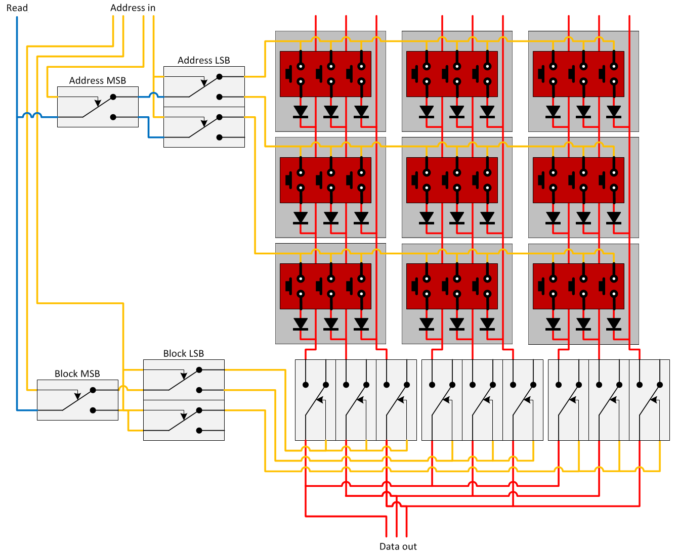
As described in the elements section, A Read Only Memory (ROM) can be seen as an universal coder. It uses dipswitches for encoding and LED’s to show address input and data output. For the address decoding, bits 0-5 are used, for the bank decoding bits 6-9. So the complete 9 bit memory address is split in two parts.
Below a circuit diagram for a reduced size memory with nine three bit words. However the 512 byte memory works exactly the same.
Capacitor RAM
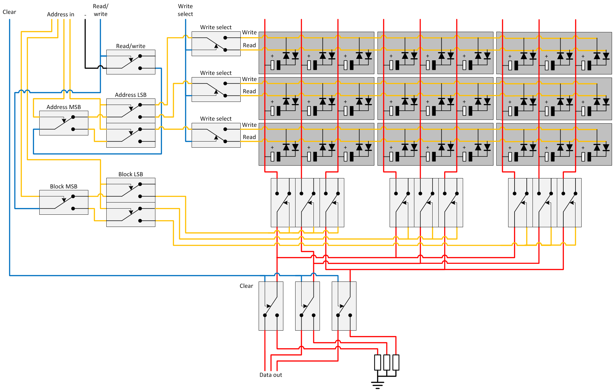
For the capacitor Random Access Memory (RAM) memory the TIM-8 memory design from Rory Mangles is used (see: www.northdownfarm.co.uk/rory/tim/tim-8.htm). In this design capacitors are used to store the bits. Each capacitor holds enough power to switch a relay on for a very brief period. However this is enough to store the bit in a memory register.
The capacitors will hold the charge (logical 1) for several hours, but will lose them in time due to internal leakage. When longer times storage are needed, this can be solved by the creation and use of a ROM subroutine that will refresh all the RAM memory cells.
The design of the RAM is very straight forward. Decoders are used to address the memory cells and select one of the eight memory banks. For clearing the memory, relays and resistors are used. For every memory address a relay is used to make a distinction between reading and writing the RAM memory.
Again a circuit diagram for a reduced size memory with nine three bit words.
Relay RAM
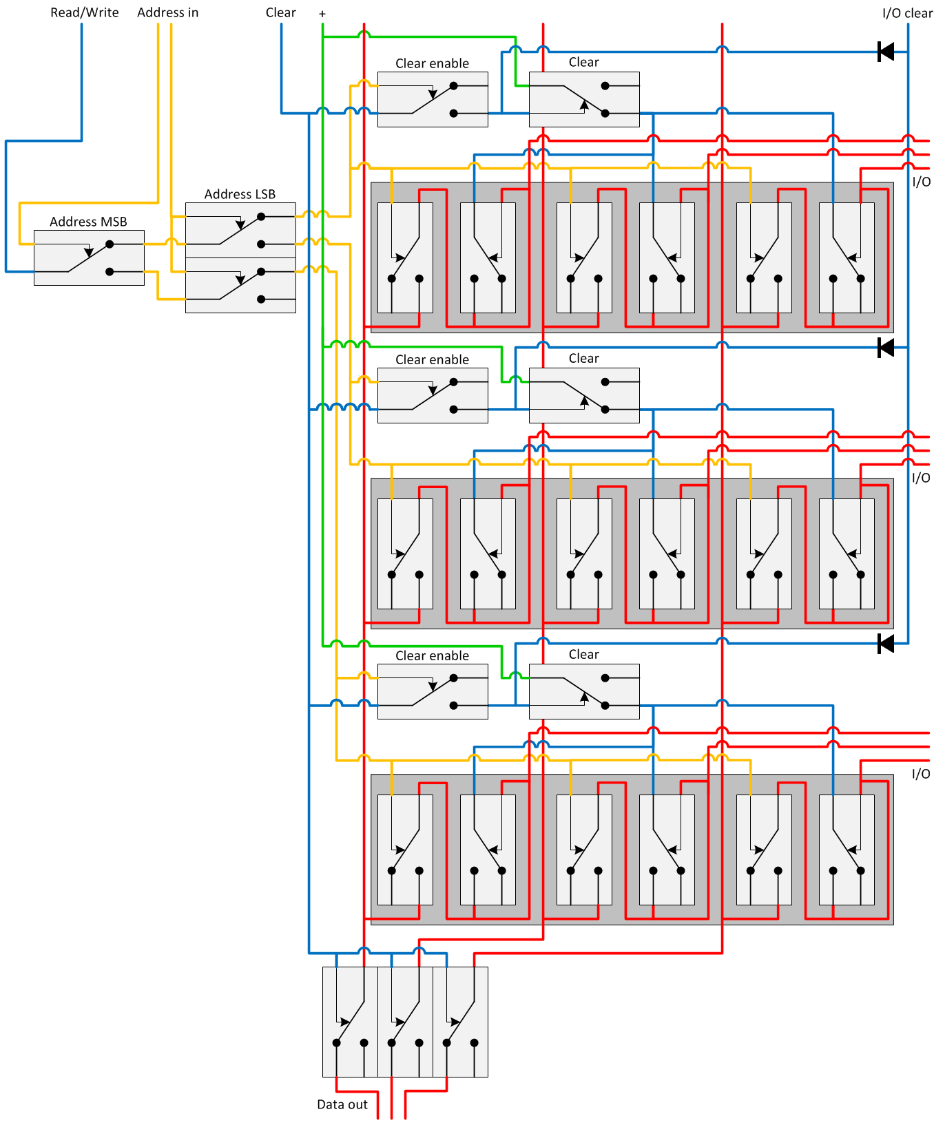
The relay RAM is used as a so called zero page memory to facilitate I/O. It is accessible via two routes: the data- and address bus as all memory does but also directly by the I/O device. Per bit two relays are used, one to store the bit and one to select the bit for reading and writing. Per memory word two relays are used to clear the word. One to switch the power off and one to select the first relay for clearing. Below a circuit diagram for a reduced size memory with three three bit words.
Memory Control
The computer treats the memory as if it is one 1024 bytes integrated memory. This is because the instruction decoder with the microcode ROM does not allow conditional processing. Therefore hardware needs to distribute addresses and control signals between the three types of memory: the memory control. This is also beneficial to reduce the power consumption of the computer. The circuit diagram of the memory control is drawn in the next figure.
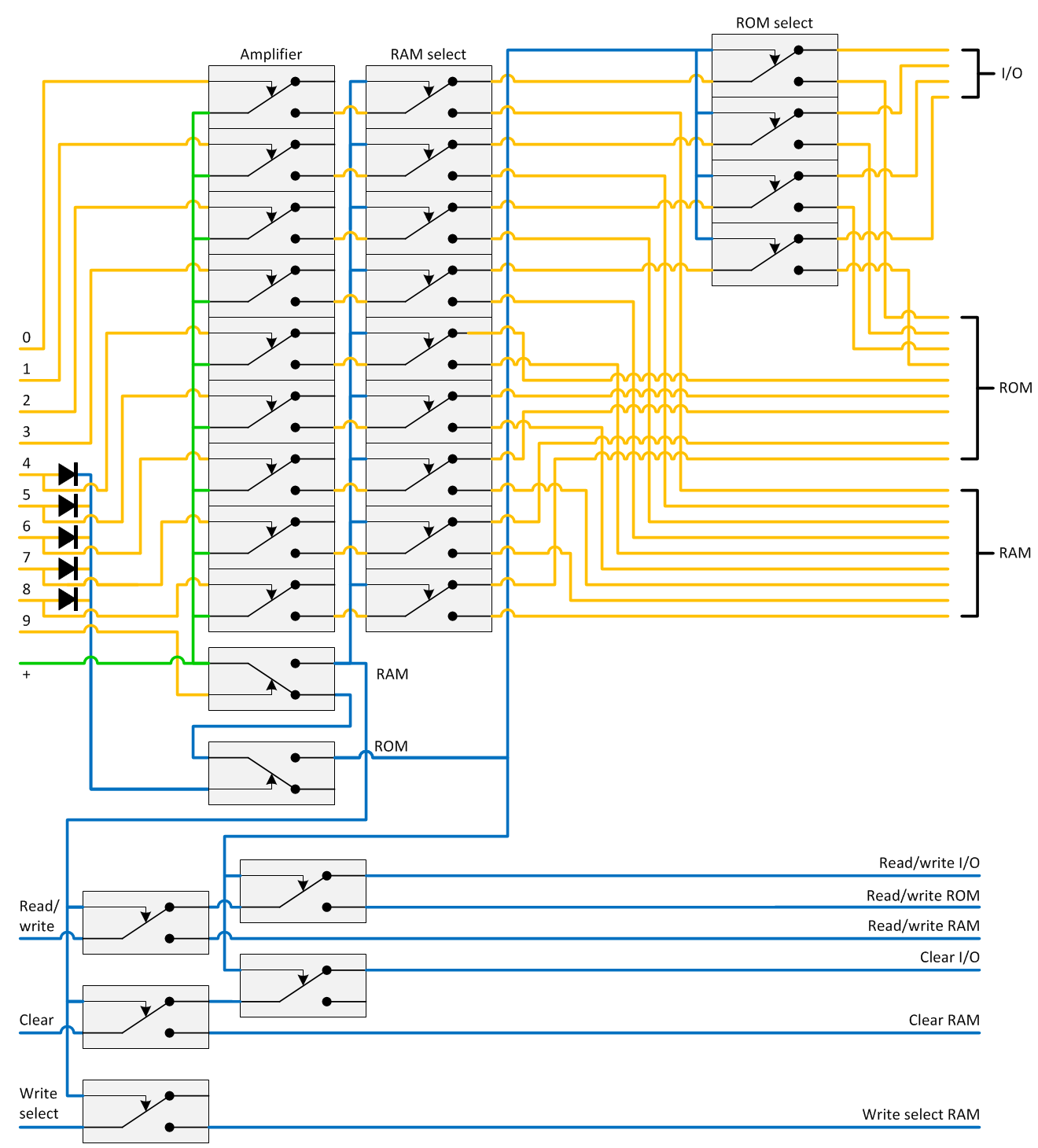
Bit 9 of the memory address distinguishes between ROM (0) and RAM (1). If bits 4-9 are 0, the I/O memory is addressed. Those two conditions make it possible to guide the memory address to one of the three types of memory (top of the circuit diagram). The bottom part of the diagram distributes the control signals to the right type of memory. Not all the control signals are needed for each memory type. For instance the ROM does not need clear or write select signals.
May 2015, Jeroen Brinkman

